- 您现在的位置:买卖IC网 > Sheet目录2006 > LTC2609CGN#PBF (Linear Technology)IC DAC 16BIT R-R QUAD 16SSOP
LTC2609/LTC2619/LTC2629
26091929fb
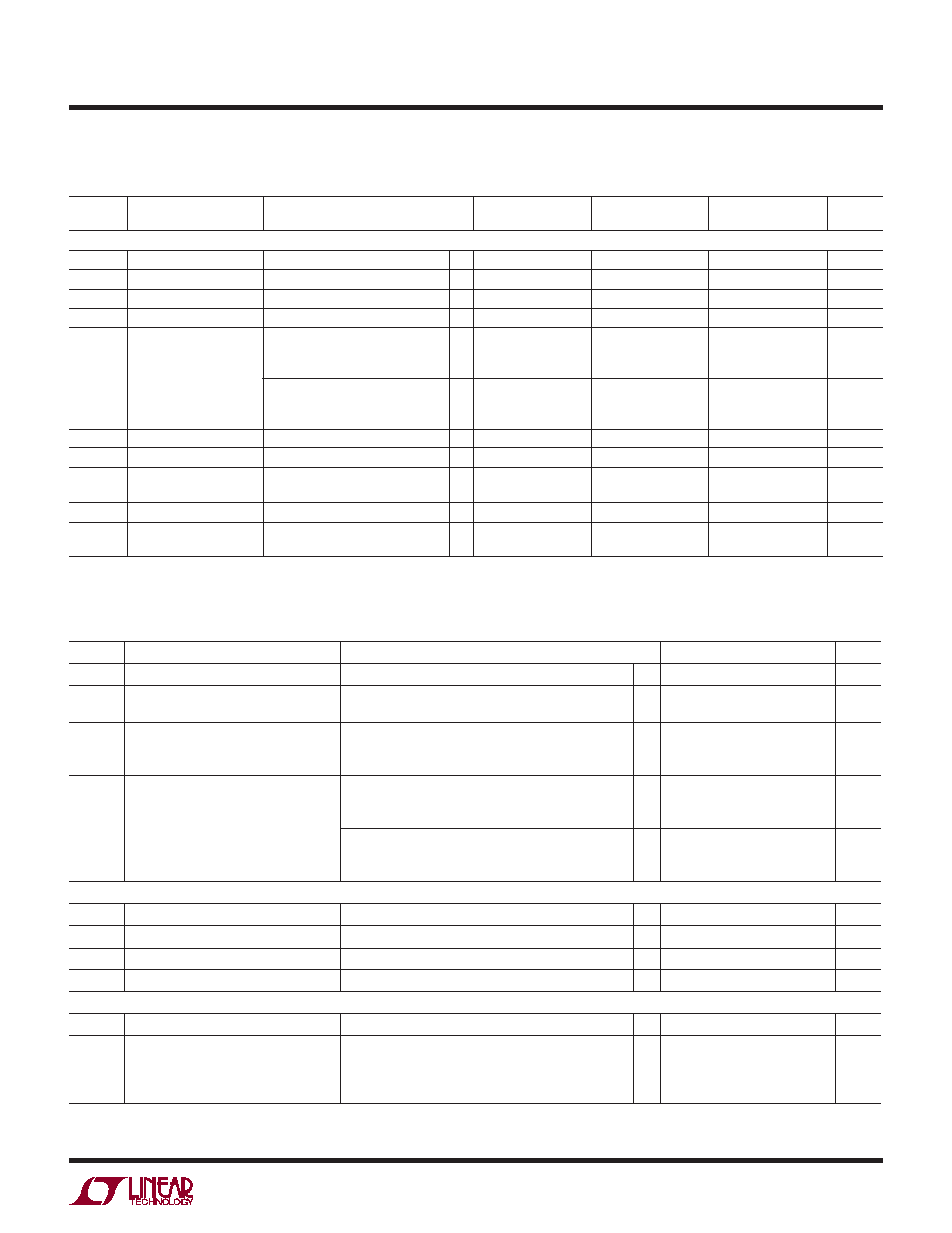
electrical characteristics The
l
denotes the specifications which apply over the full operating
temperature range, otherwise specifications are at TA = 25°C. REFA = REFB = REFC = REFD = 4.096V (VCC = 5V), REFA = REFB =
REFC = REFD = 2.048V (VCC = 2.7V). REFLO = 0V, VOUT = unloaded, unless otherwise noted.
SYMBOL PARAMETER
CONDITIONS
LTC2629/LTC2629-1 LTC2619/LTC2619-1 LTC2609/LTC2609-1
UNITS
MIN
TYP MAX MIN
TYP MAX
DC Performance
Resolution
l
12
14
16
Bits
Monotonicity
(Note 2)
l
12
14
16
Bits
DNL
Differential Nonlinearity (Note 2)
l
±0.5
±1
LSB
INL
Integral Nonlinearity
(Note 2)
l
±1
±4
±16
±64
LSB
Load Regulation
VREF = VCC = 5V, Mid-Scale
IOUT = 0mA to 15mA Sourcing
IOUT = 0mA to 15mA Sinking
l
0.02
0.125
0.1
0.5
0.3
0.4
2
LSB/mA
VREF = VCC = 2.7V, Mid-Scale
IOUT = 0mA to 7.5mA Sourcing
IOUT = 0mA to 7.5mA Sinking
l
0.04
0.05
0.25
0.2
1
0.7
0.8
4
LSB/mA
ZSE
Zero-Scale Error
Code = 0
l
1.5
9
1.5
9
1.5
9
mV
VOS
Offset Error
(Note 4)
l
±1
±9
±1
±9
±1
±9
mV
VOS Temperature
Coefficient
±6
V/°C
GE
Gain Error
l
±0.1 ±0.7
±0.1
±0.7
%FSR
Gain Temperature
Coefficient
±3
ppm/°C
The l denotes the specifications which apply over the full operating temperature range, otherwise specifications are at TA = 25°C.
REFA = REFB = REFC = REFD = 4.096V (VCC = 5V), REFA = REFB = REFC = REFD = 2.048V (VCC = 2.7V). REFLO = 0V, VOUT = unloaded,
unless otherwise noted. (Note 9)
SYMBOL PARAMETER
CONDITIONS
MIN
TYP
MAX
UNITS
PSR
Power Supply Rejection
VCC ±10%
–80
dB
ROUT
DC Output Impedance
VREF = VCC = 5V, Mid-Scale; –15mA ≤ IOUT ≤ 15mA
VREF = VCC = 2.7V, Mid-Scale; –7.5mA ≤ IOUT ≤ 7.5mA
l
0.030
0.035
0.15
Ω
DC Crosstalk (Note 10)
Due to Full-Scale Output Change (Note 11)
Due to Load Current Change
Due to Powering Down (Per Channel)
±5
±4
V
V/mA
V
ISC
Short-Circuit Output Current
VCC = 5.5V, VREF = 5.5V
Code: Zero-Scale; Forcing Output to VCC
Code: Full-Scale; Forcing Output to GND
l
15
36
60
mA
VCC = 2.7V, VREF = 2.7V
Code: Zero-Scale; Forcing Output to VCC
Code: Full-Scale; Forcing Output to GND
l
7.5
22
30
50
mA
Reference Input
Input Voltage Range
l
0
VCC
V
Resistance
Normal Mode
l
88
125
160
kΩ
Capacitance
14
pF
IREF
Reference Current, Power Down Mode DAC Powered Down
l
0.001
1
A
Power Supply
VCC
Positive Supply Voltage
For Specified Performance
l
2.7
5.5
V
ICC
Supply Current
VCC = 5V (Note 3)
VCC = 3V (Note 3)
DAC Powered Down (Note 3) VCC = 5V
DAC Powered Down (Note 3) VCC = 3V
l
1.25
1
0.35
0.15
2
1.6
1
mA
A
发布紧急采购,3分钟左右您将得到回复。
相关PDF资料
LTC2621IDD-1#PBF
IC DAC 12BIT R-R 10-DFN
LTC2630HSC6-LZ12#TRPBF
IC DAC 12BIT R-R SC70-6
LTC2642IDD-16#PBF
IC DAC 16BIT VOUT 10-DFN
LTC2704IGW-16#PBF
IC DAC 16BIT QUAD VOUT 44-SSOP
LTC2751AIUHF-16#PBF
IC DAC 16BIT CUR OUT 38-QFN
LTC2752ACLX#PBF
IC DAC 16BIT DUAL CUR OUT 48LQFP
LTC2753AIUK-16#TRPBF
IC DAC 16BIT DUAL 48-QFN
LTC2754AIUKG-16#PBF
IC DAC 16BIT QUAD IOUT 52-QFN
相关代理商/技术参数
LTC2609CGN#TRPBF
功能描述:IC DAC 16BIT R-R QUAD 16SSOP RoHS:是 类别:集成电路 (IC) >> 数据采集 - 数模转换器 系列:- 标准包装:2,400 系列:- 设置时间:- 位数:18 数据接口:串行 转换器数目:3 电压电源:模拟和数字 功率耗散(最大):- 工作温度:-40°C ~ 85°C 安装类型:表面贴装 封装/外壳:36-TFBGA 供应商设备封装:36-TFBGA 包装:带卷 (TR) 输出数目和类型:* 采样率(每秒):*
LTC2609CGN-1#PBF
功能描述:IC DAC 16BIT R-R QUAD 16SSOP RoHS:是 类别:集成电路 (IC) >> 数据采集 - 数模转换器 系列:- 标准包装:47 系列:- 设置时间:2µs 位数:14 数据接口:并联 转换器数目:1 电压电源:单电源 功率耗散(最大):55µW 工作温度:-40°C ~ 85°C 安装类型:表面贴装 封装/外壳:28-SSOP(0.209",5.30mm 宽) 供应商设备封装:28-SSOP 包装:管件 输出数目和类型:1 电流,单极;1 电流,双极 采样率(每秒):*
LTC2609CGN-1#TRPBF
功能描述:IC DAC 16BIT R-R QUAD 16SSOP RoHS:是 类别:集成电路 (IC) >> 数据采集 - 数模转换器 系列:- 标准包装:2,400 系列:- 设置时间:- 位数:18 数据接口:串行 转换器数目:3 电压电源:模拟和数字 功率耗散(最大):- 工作温度:-40°C ~ 85°C 安装类型:表面贴装 封装/外壳:36-TFBGA 供应商设备封装:36-TFBGA 包装:带卷 (TR) 输出数目和类型:* 采样率(每秒):*
LTC2609IGN#PBF
功能描述:IC DAC 16BIT R-R QUAD 16SSOP RoHS:是 类别:集成电路 (IC) >> 数据采集 - 数模转换器 系列:- 产品培训模块:Data Converter Fundamentals
DAC Architectures 标准包装:750 系列:- 设置时间:7µs 位数:16 数据接口:并联 转换器数目:1 电压电源:双 ± 功率耗散(最大):100mW 工作温度:0°C ~ 70°C 安装类型:表面贴装 封装/外壳:28-LCC(J 形引线) 供应商设备封装:28-PLCC(11.51x11.51) 包装:带卷 (TR) 输出数目和类型:1 电压,单极;1 电压,双极 采样率(每秒):143k
LTC2609IGN#TRPBF
功能描述:IC DAC 16BIT R-R QUAD 16SSOP RoHS:是 类别:集成电路 (IC) >> 数据采集 - 数模转换器 系列:- 标准包装:2,400 系列:- 设置时间:- 位数:18 数据接口:串行 转换器数目:3 电压电源:模拟和数字 功率耗散(最大):- 工作温度:-40°C ~ 85°C 安装类型:表面贴装 封装/外壳:36-TFBGA 供应商设备封装:36-TFBGA 包装:带卷 (TR) 输出数目和类型:* 采样率(每秒):*
LTC2609IGN-1#PBF
功能描述:IC DAC 16BIT R-R QUAD 16SSOP RoHS:是 类别:集成电路 (IC) >> 数据采集 - 数模转换器 系列:- 标准包装:1 系列:- 设置时间:4.5µs 位数:12 数据接口:串行,SPI? 转换器数目:1 电压电源:单电源 功率耗散(最大):- 工作温度:-40°C ~ 125°C 安装类型:表面贴装 封装/外壳:8-SOIC(0.154",3.90mm 宽) 供应商设备封装:8-SOICN 包装:剪切带 (CT) 输出数目和类型:1 电压,单极;1 电压,双极 采样率(每秒):* 其它名称:MCP4921T-E/SNCTMCP4921T-E/SNRCTMCP4921T-E/SNRCT-ND
LTC2609IGN-1#TRPBF
功能描述:IC DAC 16BIT R-R QUAD 16SSOP RoHS:是 类别:集成电路 (IC) >> 数据采集 - 数模转换器 系列:- 标准包装:2,400 系列:- 设置时间:- 位数:18 数据接口:串行 转换器数目:3 电压电源:模拟和数字 功率耗散(最大):- 工作温度:-40°C ~ 85°C 安装类型:表面贴装 封装/外壳:36-TFBGA 供应商设备封装:36-TFBGA 包装:带卷 (TR) 输出数目和类型:* 采样率(每秒):*
LTC2610CGN
功能描述:IC DAC OCTAL R-R 14BIT 16SSOP RoHS:否 类别:集成电路 (IC) >> 数据采集 - 数模转换器 系列:- 标准包装:47 系列:- 设置时间:2µs 位数:14 数据接口:并联 转换器数目:1 电压电源:单电源 功率耗散(最大):55µW 工作温度:-40°C ~ 85°C 安装类型:表面贴装 封装/外壳:28-SSOP(0.209",5.30mm 宽) 供应商设备封装:28-SSOP 包装:管件 输出数目和类型:1 电流,单极;1 电流,双极 采样率(每秒):*